Active Amplifiers & RF Switches
**DISCONTINUED**
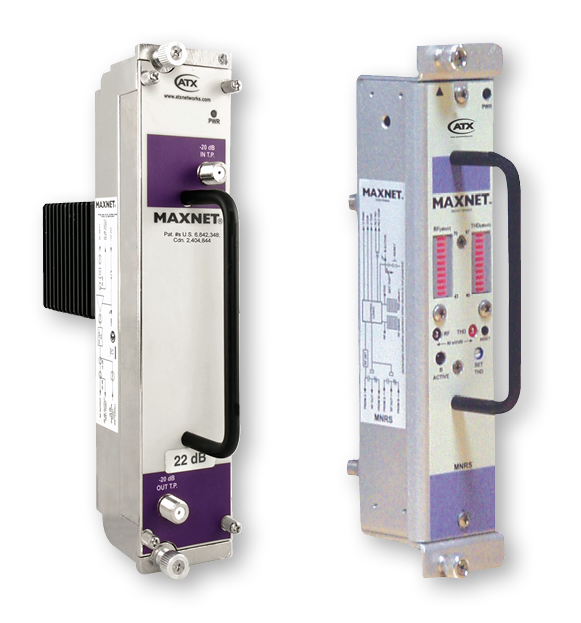
ATX offers hot-swappable MAXNET amplifiers in a variety of technologies (GaAs and GaN), as well as an RF detector/switch and a dual A/B switch.
Features
- Fully integrated, high density, modular-based platform to fit any architecture
- DOCSIS® 3.1 and CCAP™ compliant
- Removable front face for pad and EQ adjustment on most ports
- F connector
- High performance specification from 5-1002 MHz
- Hot-swappable amplifiers come in a variety of technologies (GaAs and GaN) in forward path
- Amplifiers for any application: forward combining, high gain, QAM narrowcast and return applications
- RF detector/switch accommodates redundant amplification and A/B switch applications
- Switch status indicated via front panel LED and rear terminal block relay contact
- Front panel bar graph display provides indication of RF power level and switch threshold level
- Dual A/B switch provides 2 A/B switches in 1 module with local and remote switching capabilities. Switch status indicated via front panel LED and rear terminal block relay contact
- An active chassis is required for these modules
Manufacture Discontinue (MD) MAXNET Actives and Others
**Discontinued** Data Sheet: MAXNET RF Amplifier (ANW0660)
**Discontinued** Data Sheet: MAXNET RF Switch (ANW0659)
**Discontinued** Manual: MAXNET Amplifier Installation (ANW0718)
**Discontinued** MAXNET Amplifier, RF Detector & Switch Installation Instructions (ANW0544)
**Discontinued** Manual: MAXNET RF Detector/Switch MNRS Installation (ANW0543)
*Notice of Product Discontinuation* – (FLEXNET, misc. MAXNET L-Band)
**Discontinued**
Forward Combining Amplifier
PART NUMBER | FWD. GAIN SPEC. | RESP. CONT. | INJECT. PORT | I/O T.P.
IL |
I/O
RL |
CURRENT | |||||
(Notes 1, 8, & 9) | BW (MHz) | Gain(2) (dB) | Slope(3) (dB) | Flat. (±dB) | Gain Cont. | Slope Cont. | IL (16.0±dB) | ISO(4) (dB) | (Note 6) (mA) |
||
(20.0±dB) | (Note 5) (dB) |
||||||||||
Plug-in | |||||||||||
QMN870-18GP/F* | 40-870 | 18 | -0/+1.5 | .5 | Pad | EQ | .5 | ≥ 50 | 1 | 16 | 420 |
QMN870-22GP/F* | 40-870 | 22 | -0/+1.5 | .75 | Pad | EQ | .5 | ≥ 50 | 1 | 16 | 420 |
QMN870-25GP/F* | 40-870 | 25 | -0/+1.5 | .75 | Pad | EQ | .5 | ≥ 50 | 1 | 16 | 420 |
QMN1000-18GP/F* | 40-1000 | 18 | -0/+2 | .5 | Pad | EQ | .75 | ≥ 45 | 1 | 14.5 | 420 |
QMN1000-22GP/F* | 40-1000 | 22 | -0/+2 | .75 | Pad | EQ | .75 | ≥ 45 | 1 | 14.5 | 420 |
QMN1000-25GP/F* | 40-1000 | 25 | -0/+2 | .75 | Pad | EQ | .75 | ≥ 45 | 1 | 14.5 | 420 |
Forward Combining Amplifier (cont’d)
PART NUMBER | DISTORTIONS | NOISE FIGURE | AMP TECH | ||||
(Notes 1, 8, & 9) | Output Level (dBmV) | Ch. Load (#)(10) | Ch. Slope (dB) | CTB (-dB) | CSO (-dB) | ||
(dB) | (Note 7) | ||||||
QMN870-18GP/F* | 43 | 79 | 0 | 76 | 74 | < 5.0 | PD GaAs |
QMN870-22GP/F* | 43 | 79 | 0 | 74 | 74 | < 5.0 | PD GaAs |
QMN870-25GP/F* | 43 | 79 | 0 | 74 | 72 | < 5.0 | PD GaAs |
QMN1000-18GP/F* | 43 | 79 | 0 | 76 | 74 | < 5.0 | PD GaAs |
QMN1000-22GP/F* | 43 | 79 | 0 | 74 | 74 | < 5.0 | PD GaAs |
QMN1000-25GP/F* | 43 | 79 | 0 | 74 | 72 | < 5.0 | PD GaAs |
NOTES:
Details:* = replace with I for post gain stage insertion point option.
(1) All units supplied with -20 dB F connector front input and output test point.
(2) Gain at 50 MHz.
(3) Gain at highest specified frequency.
(4) From injection port to RF input port with RF output port terminated into 75 ohm load.
(5) Worst case return loss for input and output ports.
(6) DC load current at +24 VDC.
(7) PP = Push-Pull; PD = Power-Doubled; Si = Silicon; GaAs = Gallium Arsenide.
(8) F connector mating center conductor diameter: .025” – .042”.
(9) All specifications listed include 20 dB output test point. Assume worst case of 1 dB increased insertion loss if input test point is required.
(10) 79 CW NTSC analog channels from 54-550 MHz with 320 MHz QAM loading 6 dB below analog carrier levels.
Operating temperature: 0°C to +50°C (+32°F to +122°F)
Humidity: 5-95% (without condensation)
Dimensions: 8.66”H x 1.82”W x 6.0”D (21.99H x 4.62W x 15.24D cm)
Weight: 1.9 lbs (0.96 kgs)
Forward Dual Hybrid Amplifier
PART NUMBER | FWD.GAIN SPEC. | RESP. CONT. | I/O T.P.
IL |
I/O RL | CUR. | DISTORTIONS | NOISE FIGURE | AMP TECH | |||||||
(Notes 1 and 5) | BW (MHz) | Gain (dB) | Flat.(±dB) | Gain Cont.(-dB) | Slope Cont.(-dB) | (Note 3) (mA) |
Output Level (dBmV) | Ch.Load (#)(6) | Ch.Slope (dB) | CTB(-dB) | CSO (-dB) | ||||
(20.0±dB) | (Note 2) (dB) |
(dB) | (Note 4) | ||||||||||||
QMN2870-30GP/F | 40-870 | 30 | .5 | 8 | 8 | 0.8 | 17 | 665 | 43 | 79 | 0 | 76 | 74 | 5 | PD GaAs |
QMN2870-34GP/F | 40-870 | 34 | .5 | 8 | 8 | 0.8 | 17 | 670 | 43 | 79 | 0 | 76 | 73.5 | 4.5 | PD GaAs |
QMN21000-30GP/F | 40-1002 | 30 | .7 | 8 | 8 | 1 | 15 | 665 | 43 | 79 | 0 | 76 | 74 | 5.3 | PD GaAs |
QMN21000-34GP/F | 40-1002 | 34 | .7 | 8 | 8 | 1 | 15 | 670 | 43 | 79 | 0 | 76 | 74 | 4.8 | PD GaAs |
QMN2F1000-30GP/F | 40-1002 | 30 | .7 | JXP | JXP | 1 | 15 | 665 | 43 | 79 | 0 | 76 | 74 | 5.3 | PD GaAs |
QMN2F1000-34GP/F | 40-1002 | 34 | .7 | JXP | JXP | 1 | 15 | 665 | 43 | 79 | 0 | 76 | 74 | 5.3 | PD GaAs |
NOTES:
A maximum of five forward dual hybrid amplifiers can be used in one active chassis, if it is powered with MNAC-110, MNAC-220, or MNDC power supplies.
(1) All front test points are F connectors.
(2) Worst case return loss for input and output ports.
(3) DC load current (worst case) at +24 VDC.
(4) PP = Push-Pull; PD = Power-Doubled; Si = Silicon; GaAs = Gallium Arsenide
(5) F connector mating center conductor diameter: .025” – .042”.
(6) 79 CW NTSC analog channels from 54-550 MHz with 320 MHz QAM loading 6 dB below analog carrier levels.
Operating temperature: 0°C to +50°C (+32°F to +122°F)
Humidity: 5-95% (without condensation)
Dimensions: 8.66”H x 1.82”W x 6.0”D (21.99H x 4.62W x 15.24D cm)
Weight: 1.9 lbs (0.96 kgs)
High Gain Amplifier
QMN21000-41PHF | QMN2F1000-42PHF | ||
MEASUREMENT | FREQUENCY | QA | QA |
GAIN | 50-1002 MHz | 41 +/- 1.0 dB | 42 +/- 1.0 dB |
RETURN LOSS | 50-1002 MHz | ≥ 14.5 dB | |
INPUT PAD | 50-1002 MHz | MN_PAD(1) | MN_PAD(1) |
GAIN CONTROL | 50-1002 MHz | 10 (-dB) | MN_PAD(1) |
SLOPE CONTROL (-dB) | 50-1002 MHz | 8 (-dB) | QAE_EQ(2) |
TEST POINT | 50-1002 MHz | 20 +/- 1.0 dB | |
NOISE FIGURE | 50-1002 MHz | < 4.5 dB | |
INPUT CURRENT | DC | 730mA @ 24 VDC(3) | |
POWER CONSUMPTION | DC | 17W | |
OPERATING TEMPERATURE | 0°C to +50°C (+32°F to +122°F) | ||
HUMIDITY | 5-95% (without condensation) | ||
DIMENSIONS | 8.66”H x 1.82”W x 6.0”D (21.99H x 4.62W x 15.24D cm) | ||
WEIGHT | 1.9 lbs (0.96 kg) | ||
DIGITAL PERFORMANCE | MOSTLY DIGITAL(4) | ||
---|---|---|---|
REF OUTPUT MAX./QAM 256 | 43 dBmV(5) | ||
MINIMUM INPUT POWER/CH | -2 dBmV QAM 256, +10 dBmV Analog(6) | ||
MINIMUM MER AT REF OUTPUT | 40 dB | ||
BER BEFORE/AFTER AMP(7) | < 1E-9 |
NOTES:
(1) Ships with MN0PAD. See page 6.
(2) Ships with 0 dB QAE EQ. See page 6.
(3) A maximum of five forward high gain amplifiers can be used in one active chassis, if it is powered with MNAC-110, MNAC-220, or MNDC power supplies.
(4) Tested with 150x QAM 256 channels up to 1002 MHz at specified output power, as well as 4 CWs @ +6 dB output relative to QAMs to simulate pilot channels.
(5) See chart for other maximum output ratings for the number of QAM channels.
(6) If any analog channels present then they should be ≥ 10 dBmV to avoid CNR impacts.
This means min. QAM level would be -6 dB relative. If all QAM channels, then QAMs may be as low as -2 dBmV/ QAM 256.
(7) Pre-FEC BER. Results show no detectable bit errors if operated within recommended range.
*DISCONTINUED*-Narrowcast QAM Amplifier
PART NUMBER | # AMPS. | GAIN SPECIFICATIONS | OUT. T.P. | RETURN LOSS | ||||||
BW (MHz) | Gain(3) | Flat.(4)
(±dB) |
Input (MHz) | Output | ||||||
870 MHz (dB) | 500 MHz (±dB) | 54 MHz (±dB) | (20±dB)
(Note 2) |
54-500 MHz (≥dB) | 500-870 MHz (≥dB) | 54-870 MHz (≥dB) | ||||
(Note 1) | ||||||||||
QMNN1-13P* | Single | 54-870 | 13 | 0.5 | 1 | 0.2 | 1 | 16 | 16 | 16 |
QMNN2-13P* | Dual | 54-870 | 13 | 0.5 | 1 | 0.2 | 1 | 16 | 16 | 16 |
QMNN1-17P* | Single | 54-870 | 17 | 0.5 | 1 | 0.2 | 1 | 16 | 16 | 16 |
QMNN2-17P* | Dual | 54-870 | 17 | 0.5 | 1 | 0.2 | 1 | 16 | 16 | 16 |
QMNN1-21P* | Single | 54-870 | 21 | 0.5 | 1 | 0.2 | 1 | 16 | 16 | 16 |
QMNN2-21P* | Dual | 54-870 | 21 | 0.5 | 1 | 0.2 | 1 | 16 | 16 | 16 |
*DISCONTINUED*-Narrowcast QAM Amplifier (cont’d)
PART NUMBER | IMAX | NOISE FIG. | REV.ISO. | OUTPUT LEVEL w MER >43 dB & Pre BER <10^-10 |
|||
@24V (mA) | QAM Channel Loading 550-870 MHz(5)(7) | ||||||
(dB) | (dB) | 1 (dBmV) | 2 (dBmV) | 4 (dBmV) | 8 (dBmV) | ||
(Note 1) | |||||||
QMNN1-13P* | 175 | 6 | 20 | +63 | +57 | +51 | +47 |
QMNN2-13P* | 350 | 6 | 20 | +63 | +57 | +51 | +47 |
QMNN1-17P* | 175 | 6 | 23 | +64 | +58 | +52 | +48 |
QMNN2-17P* | 350 | 6 | 23 | +64 | +58 | +52 | +48 |
QMNN1-21P* | 175 | 6 | 26 | +64 | +58 | +52 | +48 |
QMNN2-21P* | 350 | 6 | 26 | +64 | +58 | +52 | +48 |
NOTES:
(1) * = F for F connectors or B for BNC connectors.
(2) All front test points are F connectors. F connector mating center conductor diameter: .025” – .042”.
(3) Gains at 500 MHz and 50 MHz are referenced to the gain at 870 MHz.
(4) As measured over any consecutive 6 MHz bandwidth.
(5) All QAM channels adjacent.
(6) QAM signal(s) performance at input: MER > 45 dB and Pre BER < 10^-10.
(7) QAM signal(s) output performance: MER > 43 dB and Pre BER < 10^-10.
Operating temperature: 0°C to +50°C (+32°F to +122°F)
Humidity: 5-95% (without condensation)
Dimensions: 8.66”H x 1.82”W x 6.0”D (21.99H x 4.62W x 15.24D cm)
Weight: 1.9 lbs (0.96 kg)
Return Amplifier
PART NUMBER | GAIN SPEC. | RESP. CONT. | I/O T.P.
IL |
I/O RL |
CURRENT | DISTORTIONS | NOISE FIGURE | AMP TECH | ||||||||
(Notes 1 & 2) | BW (MHz) | Gain(3) (dB) | Slope(4) (dB) | Flat. (±dB) | Gain Cont. | Slope Cont. | (Note 6) (mA) | Output Level (dBmV) | Ch. Load (#) | Ch. Slope (dB) | CTB (-dB) | CSO (-dB) | ||||
Plug-in | (20.0±dB) | (Note 5) (dB) |
(dB) | (Note 7) | ||||||||||||
QMN200-22/F | 5-200 | 22 | -1/+.5 | .5 | Pad | EQ | .5 | 18 | 220 | 50 | 22 | 0 | 70 | 74 | 5 | PP Si |
QMN200-28L/F | 5-200 | 28 | -1/+.5 | .5 | Pad | EQ | .5 | 18 | 140 | 50 | 10 | 0 | 67 | 70 | 5 | PP Si |
NOTES:
(1) F connector mating center conductor diameter: .025” – .042”.
(2) All specifications listed include 20 dB output test point. Assume worst case of 1 dB increased insertion loss if input test point is required.
(3) Gain at 5 MHz.
(4) Gain at highest specified frequency.
(5) Worst case return loss for input and output ports.
(6) DC load current at +24 VDC.
(7) PP = Push-Pull; PD = Power-Doubled; Si = Silicon; GaAs = Gallium Arsenide.
Operating temperature: 0°C to +50°C (+32°F to +122°F)
Humidity: 5-95% (without condensation)
Dimensions: 8.66”H x 1.82”W x 6.0”D (21.99H x 4.62W x 15.24D cm)
Weight: 1.9 lbs (0.96 kg)
RF Detector/Switch
MNRSF REDUNDANT AMPLIFIER CONFIGURATION |
MNRSF RF DETECTOR A/B SWITCH CONFIGURATION |
|
RF (5-1000 MHz) | ||
INSERTION LOSS (Max) | 2.3 dB(1) | 2.3 dB / 1.5 dB(3) |
INPUT/OUTPUT RETURN LOSS (Min) | 18 dB | 18 dB |
ISOLATION (Min) | 70 dB(2) | 70 dB |
OPERATIONAL | ||
COMPOSITE RF POWER RANGE | 40-70 dBmV | |
SWITCH THRESHOLD RANGE | 37-67 dBmV | |
SWITCH THRESHOLD CONTROL | Font Panel Control | |
SWITCH TIME (Max) | 10mS | |
SWITCH STATUS INDICATION | Front Panel LED & Rear NO Contact | |
OPERATING TEMPERATURE | -40ºC to +60ºC (-40ºF to +140ºF) | |
ELECTRICAL | ||
INPUT VOLTAGE | 24V | |
INPUT CURRENT | 70mA | |
POWER INDICATOR | Front Panel LED | |
OTHER | ||
HUMIDITY | 5-95% (without condensation) | |
DIMENSIONS | 8.6”H x 1.75”W x 2.5”D (21.84H x 4.45W x 6.35D cm) | |
WEIGHT | 1.04 lbs (0.47 kg) | 1.06 lbs (0.48 kg) |
NOTES:
(1) Input section < 0.5 dB; Output section < 1.8 dB.
(2) Isolation measured between primary (A) and secondary (B) paths.
(3) Loss for A/B (0.8 dB allowance for coupler).
Rear Panel Terminal Block Assignment
TB# | RF DETECTOR / SWITCH |
---|---|
1 | V PWR |
2 | COM |
3 | V THD |
4 | RLY COM |
5 | RLY NO |
Dual A/B Switch
MNDABF | |
RF (5-870 MHz) | |
INSERTION LOSS (Max) | 0.5 dB |
INPUT/OUTPUT RETURN LOSS (Min) | 18 dB |
ISOLATION (Min) | 60 dB |
OPERATIONAL | |
SWITCH TRANSFER CONTROL | Front Panel Pushbutton or Remote Pulsed Logic Signal (5-24 VDC) |
SWITCH TRANSFER TIME | < 10mS |
SWITCH STATUS INDICATION | Front Panel LED and Rear TB NO Contact |
OPERATING TEMPERATURE | -40ºC to +60ºC (-40ºF to +140ºF) |
ELECTRICAL | |
INPUT VOLTAGE | 24V |
INPUT CURRENT | 70mA |
POWER INDICATION | Front Panel LED |
OTHER | |
HUMIDITY | 5-95% (without condensation) |
DIMENSIONS | 8.6”H x 1.75”W x 2.5”D (21.84H x 4.45W x 6.35D cm) |
WEIGHT | 1.06 lbs (0.48 kg) |
Rear Panel Terminal Block Assignment
TB# | DUAL A/B SWITCH |
---|---|
1 | SW1 IN |
2 | SW1 RLY NO |
3 | COM |
4 | SW2 RLY NO |
5 | SW2 IN |
**Discontinued**
Forward Combining Amplifier
Part Number | Description |
---|---|
QMN870-18GP/F | 870 MHz, 18 dB, GaAs PD, F Connectors, 20 dB Input and Output TPs |
QMN870-22GP/F | 870 MHz, 22 dB, GaAs PD, BNC Connectors (rear only), 20 dB Input and Output TPs |
QMN870-25GP/F | 870 MHz, 25 dB, GaAs PD, F Connectors, 20 dB Input and Output TPs |
QMN1000-18GP/F | 1000 MHz, 18 dB, GaAs PD, F Connectors, 20 dB Input and Output TPs |
QMN1000-22GP/F | 1000 MHz, 22 dB, GaAs PD, F Connectors, 20 dB Input and Output TPs |
QMN1000-25GP/F | 1000 MHz, 25 dB, GaAs PD, F Connectors, 20 dB Input and Output TPs |
Forward Dual Hybrid Amplifier
Part Number | Description |
---|---|
QMN2870-30GP/F | 870 MHz, 30 dB, GaAs PD, F Connectors |
QMN2870-34GP/F | 870 MHz, 34 dB, GaAs PD, F Connectors |
QMN21000-30GP/F | 1002 MHz, 30 dB, GaAs PD, F Connectors |
QMN21000-34GP/F | 1002 MHz, 34 dB, GaAs PD, F Connectors |
QMN2F1000-30GP/F | 1002 MHz, 30 dB, GaAs PD, JXP Fixed Gain/Slope Adjust(1), F Connectors |
QMN2F1000-34GP/F | 1002 MHz, 34 dB, GaAs PD, JXP Fixed Gain/Slope Adjust(1), F Connectors |
NOTE:
(1) Use MN*PAD and MN*EQ for gain and slope adjust in “Fixed” adjustment amplifiers.
High Gain Amplifier
Part Number | Description |
---|---|
QMN21000-41PHF | 1002 MHz, 41 dB, GaN PD, F Connectors |
QMN2F1000-42PHF | 1002 MHz, 42 dB, GaN PD, F Connectors, Plug-in Pad/EQ |
Return Amplifier
Part Number | Description |
---|---|
QMN200-22F | 200 MHz, 22 dB, Si PP, F Connectors, 20 dB Input and Output TPs |
QMN200-28LF | 200 MHz, 28 dB, Si PP, Low Current, F Connectors, 20 dB Input and Output TPs |
RF Detector/Switch
Part Number | Description |
---|---|
MNRSDF | RF Detector / Switch with Switch Delay and Level Modification |
MNRSF | RF Detector / Switch, F Connectors |
MNRSLF | RF Detector Switch with Low Level Mod (25-55 dBmV) |
Dual A/B switch
Part Number | Description |
---|---|
MNDABF | Dual A/B Switch, F Connectors |